Photolithography uses three basic process steps to transfer a pattern from a mask to a wafer: coat, develop, expose. The pattern is transferred into the wafer’s surface layer during a subsequent process.
How does photo lithography work?
Photolithography is a patterning process in which a photosensitive polymer is selectively exposed to light through a mask, leaving a latent image in the polymer that can then be selectively dissolved to provide patterned access to an underlying substrate.
Why is photolithography used?
Photolithography is one of the most important and easiest methods of microfabrication, and is used to create detailed patterns in a material. In this method, a shape or pattern can be etched through selective exposure of a light sensitive polymer to ultraviolet light.
How many steps of photo resist processing and what are they?
Photoresist processing, or simply resist processing, basically consists of six steps: 1) dehydration and priming; 2) resist coating; 3) soft baking; 4) exposure; 5) development; and 6) post-development inspection.
What is photolithography in nanotechnology?
Photolithography is the process of defining a pattern on the surface of a device material slice. By sequentially using such patterns to define metal contacts or etched areas a complete device is gradually built up.
What is Lithography in MEMS?
Lithography in the MEMS context is typically the transfer of a pattern to a photosensitive material by selective exposure to a radiation source such as light. A photosensitive material is a material that experiences a change in its physical properties when exposed to a radiation source.
What is photolithography masking?
A photolithography mask is an opaque plate or film with transparent areas which allows light to shine through a defined pattern. They are commonly used in photolithography processes, but are also used in many other applications by a wide range of industries and technologies, notably microfluidics.
What are the two processes involved in photolithography?
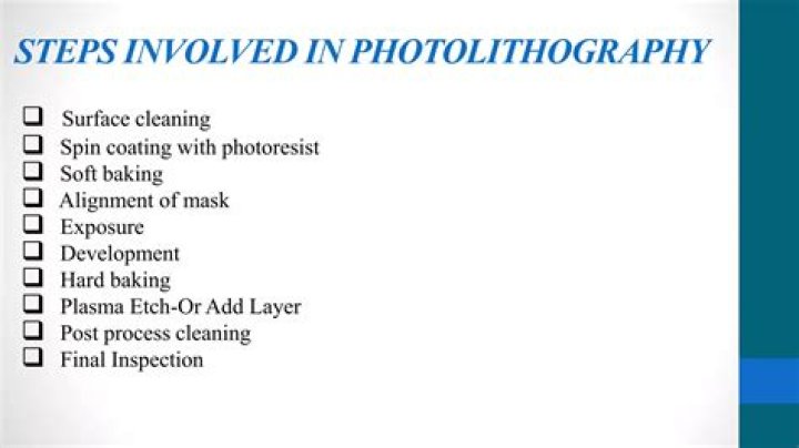
Photolithography is the process of transferring geometric shapes on a mask to the surface of a silicon wafer. The steps involved in the photolithographic process are wafer cleaning; barrier layer formation; photoresist application; soft baking; mask alignment; exposure and development; and hard-baking.
Steps of Photolithography – Coat, Expose, Develop There are three basic steps to photolithography: Coat – A photosensitive material (photoresist or resist) is applied to the substrate surface. Expose – The photoresist is exposed using a light source, such as Near UV (Ultraviolet), Deep UV or X-ray.
What is the lithography process of photoresist?
The overall lithography process is summarized in \\fgure 2. After the pattern is formed on the photoresist and the wafer surface is exposed (developing process) the exposed wafer surface is etched. It is also possible to deposit material on the exposed surface. 2
What is lithography and how does it work?
• Lithography is the transfer of geometric shapes on a mask to a smooth surface. • The process itself goes back to 1796 when it was a printing method using ink, metal plates and paper. • In modern semiconductor manufacturing,
What is the role of lithography in the IC wafer fabrication process?
Lithography is also used to expose certain parts of the wafer surface for doping (either with a hard mark for thermal diusion or with a soft mask for ion implantation). The correct placement of the circuit pattern involves alignment or registration of various masks. An IC wafer fabrication process can require forty or more patterning steps.